PCB
PCB
Blog Article
High-Density Interconnect (HDI) PCBs: The Backbone of Advanced Electronics
In the fast-paced world of electronics, where devices are becoming increasingly compact and powerful, High-Density Interconnect (HDI) Printed Circuit Boards (PCBs) have emerged as a critical enabler of innovation. HDI PCBs are revolutionizing the way electronic devices are designed and manufactured, allowing for greater miniaturization, enhanced performance, and increased functionality. In this article, we delve into the intricacies of HDI PCB technology, its applications, and its impact on the electronics industry. Expand your knowledge on HDI PCB manufacturer.
The Evolution of HDI PCB Technology
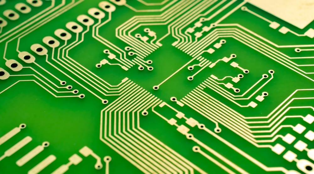
HDI PCB technology represents a significant evolution from traditional PCB manufacturing processes. While conventional PCBs typically feature through-hole vias and larger trace widths, HDI PCBs leverage advanced techniques to achieve higher wiring densities and finer features. Key innovations in HDI PCB technology include microvias, sequential lamination, and fine-pitch components, which enable designers to pack more functionality into smaller form factors.
Key Features of HDI PCBs
1. Microvias: Microvias are small holes drilled into PCB substrates, typically with diameters ranging from a few micrometers to several hundred micrometers. These microvias allow for the routing of high-density traces between layers, facilitating more compact designs and shorter signal paths.
2. Sequential Lamination: HDI PCBs often utilize sequential lamination processes, where multiple layers of conductive and insulating materials are laminated together in a step-by-step fashion. This allows for precise alignment of vias and traces, as well as the creation of complex, multi-layered structures.
3. Fine-Pitch Components: HDI technology enables the integration of fine-pitch components with smaller footprints and tighter pin spacings. This allows for increased component density and improved functionality within limited space constraints.
4. Increased Routing Density: By leveraging microvias and fine-pitch components, HDI PCBs achieve higher routing densities compared to traditional PCBs. This results in improved signal integrity, reduced electromagnetic interference, and enhanced overall performance.
Advantages of HDI PCBs
1. Miniaturization: HDI PCBs enable the creation of smaller, lighter, and more compact electronic devices. This is particularly advantageous in applications where space is limited, such as smartphones, tablets, and wearable devices.
2. Enhanced Performance: With shorter signal paths, reduced parasitic capacitance, and optimized trace geometries, HDI PCBs offer superior electrical performance. This translates to faster data transfer rates, lower power consumption, and increased reliability in high-speed and high-frequency applications.
3. Design Flexibility: HDI technology provides designers with greater flexibility in PCB layout and component placement. Designers can achieve higher levels of integration, implement complex routing schemes, and optimize signal paths for maximum performance and efficiency.
4. Cost Efficiency: While HDI technology initially involved higher fabrication costs due to its complexity, advancements in manufacturing processes and economies of scale have made it increasingly cost-effective. The benefits of improved performance and miniaturization often outweigh the additional manufacturing costs, making HDI PCBs a viable option for a wide range of applications.
Applications of HDI PCBs
HDI PCBs find applications across various industries and sectors, including:
- Consumer Electronics: Smartphones, laptops, tablets, and wearables benefit from the compact size and high performance of HDI PCBs.
- Automotive Electronics: Advanced driver-assistance systems, infotainment systems, and automotive sensors rely on HDI technology for reliable operation in harsh environments.
- Aerospace and Defense: Avionics, radar systems, and satellite communications systems utilize HDI PCBs for their ruggedness, reliability, and high-performance capabilities.
- Medical Devices: Medical imaging equipment, patient monitoring systems, and implantable devices leverage HDI technology for compact designs and precise functionality.
Future Trends in HDI Technology
As the demand for smaller, more powerful electronic devices continues to grow, several trends are shaping the future of HDI PCB technology:
- Advanced Materials: The development of new materials with enhanced electrical, thermal, and mechanical properties is enabling further miniaturization and performance improvements in HDI PCBs.
- Embedded Components: Integration of passive and active components directly into the PCB substrate is emerging as a trend, reducing board size, improving signal integrity, and simplifying assembly processes.
Conclusion
High-Density Interconnect (HDI) PCB technology has become indispensable in the design and manufacture of advanced electronics. With their compact size, enhanced performance, and design flexibility, HDI PCBs are driving innovation across various industries. As technology continues to advance, HDI technology will remain at the forefront of electronics manufacturing, enabling the development of smaller, more powerful, and more sophisticated electronic devices.
Report this page